Schematics and details for open decoder (var. 2)
- Schematic:
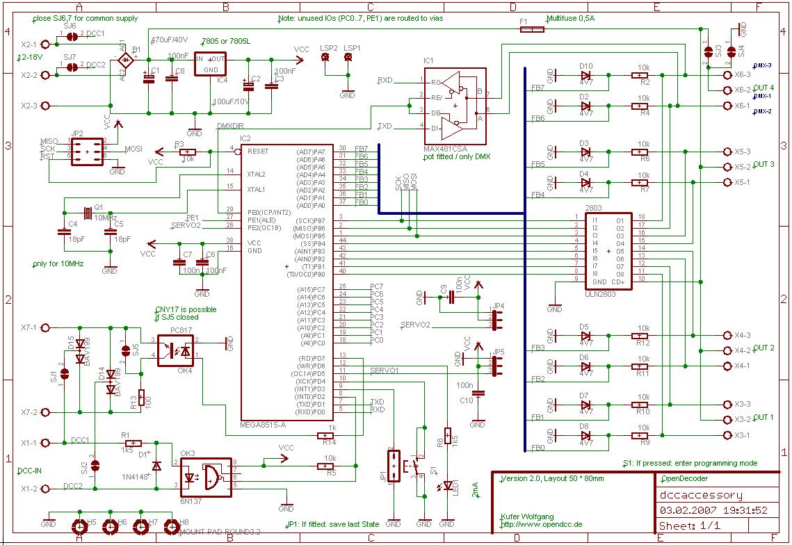
The low-cost decoder 1 reaches its limit when more complex tasks are to be performed, the decoder platform 2 based on an ATmega8515 with 8K Flash, 512 bytes RAM and 512 bytes of EEPROM was created.
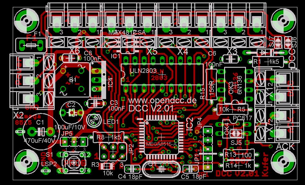
For space and cost reasons this platform is partly built in SMD (but still with moderately large components which could be manually soldered).
Schematic V2.01 (V2.00)
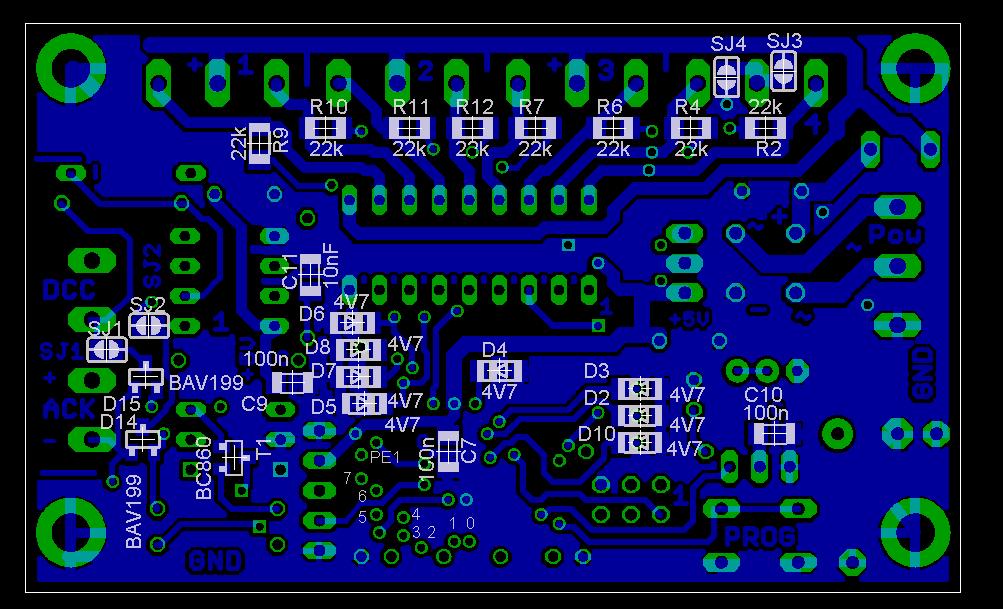
There is also a version without SMD. This version is called 2.1, slightly larger (80 * 100 mm) and equipped with dual drivers (to 1A load), but runs with the same software. - Circuit description:
Power supply:
The input voltage of the external power supply is fed to X2 (15V), type of current(AC/DC) or polarity does not matter, therefore a model train transformer, a power adapter or the DCC signal can be used. The signal DCC can be also passed along on the board itself without external bridge by closing solder jumpers SJ6 and SJ7. The input voltage is rectified and by means of the usual 7805 series regulator the 5V for the processor are generated. The idle current is about 20mA, both the T0220 and the smaller T039 can be fitted.
Note 1: I've noticed that some of Roco turnouts only switch at 15V, in this case due to the voltage drops across the rectifier and output driver the supply voltage need to be increased to 16V AC or 18V DC.
Note 2: If only servos or DMX will be controlled, then a lower supply voltage of 7-9V makes life much easier for the 7805. I use here plug power supplies, which are 'cheap' at the next recycling centre.
DCC input:
The DCC signal is connected to X1. It is separated from the voltage supply of the decoder via an optocoupler (6N136). The optocoupler ensures a trouble-free operation even in large systems. 6N136 as well as 6N137 or 4N25 can be used. With 6N137, in addition, the Pin 7 (enable input) must be connected to pin 8 (this is not in the layout, because this pin must remain free when 6N136 is used).
Tip: if you want to monitor the DCC input signal the free wheeling diode can be replaced with a LED.
The 4N25 (or its derivatives) must be mounted as follows: pin 1 of the 4N25 connects to pin 2 of the layout (thus pin 1 of the layout remains unconnected). The 4N25 is relatively slow; in particular the release time is relatively long. The pull-up (R5) at the output must be scaled down to 1k, otherwise there are only distorted signals after the optocoupler.
Recommendation: Use 6N136.
R15 and C11 are not fitted.
Switching output:
Here the usual ULN2803 is used with a DIL package so that it can be easily socketed. This driver can deliver 0.5A continuous current per output; it is internally equipped with a free-wheeling diode for inductive loads. The outputs are combined in groups of three terminals to allow for an easy installation
If the output current is not sufficient, the following trick can be applied: simply solder a second ULN2803 piggyback on the first chip.
Switching of inductive loads:
Turnouts are usually driven by coils and are equipped with a final position turnoff-contact in the drive. The final disconnection causes an induction tension which flows backwards the the driver and is conducted by the integrated free-wheeling diode. If this switch "flutters" and turns on and off repeatedly quickly in a short time, it can happen that the free-wheeling diode is overloaded before the trip point of the polyfuse.
In such a case, remedy can be created with a transient voltage suppression diode across the coil - but better replace the turnout drive.
Moreover, the turning-off causes a significant field in this area - therefore turnout wiring may not be long, they should also not be routed parallel to other cables and should be twisted.
Processor:
The processor is an Atmel ATmega8515.
Clock generation:
The Atmel ATmega8515 is supplied with a RC oscillator that runs at 8 MHz, the crystal and the capacitors can be omitted. The hex file to be loaded must match for this frequency, so if this value is set during compilation (F_CPU) to 8,000,000, all timing settings are adjusted automatically.
Note: the timing accuracy is specified by Atmel with 3%, which is sufficient for this application. Although under extremely unfavourable combination of clock deviation, temperature, supply voltage, delays in the optocoupler _and_ a DCC signal on the edge of the allowable timing a malfunction can happen.
If you prefer to be hyper precise, you can fit a crystal (and the additional 18pF capacitors). However, a hex file for the selected frequency must also be loaded. Of course, during compilation a value (F_CPU) in accordance with the clock rate must be provided, all the timing settings are adjusted automatically. Also processor fuse bits must be changed accordingly to "external crystal".
Button and LED:
As LED use a 2mA types, it can be driven directly by the ATmega. The button is used to start the programming.
Servo control:
2 slots for servos are provided, the usual pinout GND - +5V - Control is used. The servos are always supplied with +5V and depending on the setup, the control signal is turned on or off when not moving. Some servos (especially cheap ones) generate rather violent current surges from the 5V supply and also feed back load dumps. To intercept this surges a large ceramic block capacitors (C9 and C10) at the servo port of 22uF ... 47uF should be used. If these capacitors are not available in ceramic, one can also use a ceramic capacitor 100nF and piggyback an electro-capacitors which should have a dielectric strength of at least 10V. High performance servos (eg for a drawbridge) must be provided with separate power supply.
The servos occupy separate outputs to the processor (on timers), so that the activation caused little CPU load.
Turnout feedback:
The switching outputs of the turnout are fed back through resistor and zener diode on inputs. Here, the position of the end switch contact can be queried. This is a confirmation of actual turnout real position and so whether the turnout has switched can be detected.
Important: these resistors should be fitted only if a feedback decoder is to be built, they interfere with a control LED! When used instead of a end micro switch contact or photocell, the feedback inputs must be connected directly. You just have to add an additional small breadboard with pin connectors and wired from there as follows:Direct feedback input Switch 1 Port PA0 Connection with cathode of diode D8 Switch 2 Port PA2 Connection with cathode of diode D6 Switch 3 Port PA4 Connection with cathode of diode D4 Switch 4 Port PA6 Connection with cathode of diode D2
This feedback contacts connect to ground, the corresponding pull-up is already integrated OpenDecoder2.
DMX:
A bi-directional RS485 Drivers (switchable online) allows both the control of the board of DMX and the generation of the DMX data stream Together with the mouse OpenDCC macro programming can allow to switch the background lighting of the model train DCC .
Acknowledge pulse and / or emergency shutdown:
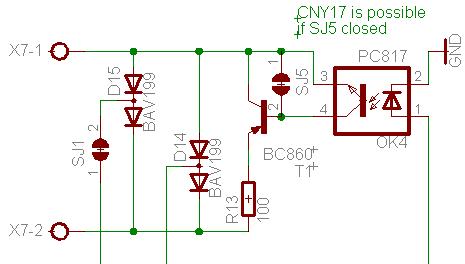
OpenDecoder V2 has the ability to report something back to the Central station. This can be either a DCC-compliant Acknowledge pulse, a pulse on a separate acknowledgment line or an emergency stop, which is reported via a separate line.- DCC compliant Acknowledge pulse:
these are short-term increase in load (> 60 mA for 6 ms) on the DCC input. These pulses can be evaluated by the central station on the programming track. For this purpose, a switchable load of 100 ohms is applied by SJ1 and SJ2 (SJ = solder jumper) and diodes (BAV199) to the DCC signal. X7 in this case is not used. - Separate feedback pulse:
Here all X7 exits of the decoders (Pin 1 = Ground) are simply combined with a Pullup (e.g., 4k7 or integrated in the head office OC). Then the return registration pulse must be read directly in the central station. In this case The diodes can be omitted and SJ1 / 2 stays open. - Emergency stop for non-switching turnout :
In the same ring line and circuit as above, a shutdown of the model (or parts thereof) is triggered. This can be either direct (emergency) or via a feedback system (eg S88).
- DCC compliant Acknowledge pulse:
- Motor Control: For the control of motor drives,
one must convert the pulses to a signal with reversing polarity, this polarity switch
or a transistor level converter can be used.
For combined decoder (light / sound / movement) as for the coffee cup carousel, there is a daughterboard, that contains either a full engine power amplifier (with an H-bridge) or a simple circuit a transistor for PWM control and a subsequent pole reversal relay. This board is plugged into JP1 and JP4.
There are also applications for such OpenDCC Animat with 2 integrated H-bridges. - Layout:
The board is implemented in version 2.0 as a double-sided circuit board with dimensions of 80 * 50mm. There are only a few SMDs, mostly through-hole components and DIL ICs used, a reduction is possible. Enough space for large screw and mounting holes are provided so that the finished decoders are easily installed.
Component side
Solder side
How does the CV programming works?
If the decoder has detected a valid CV programming process and a
feedback is required to the central station, then a so-called Service Mode acknowledge is triggered.
These must be presented to the central station, by 6ms long load increase of at least 60mA.
This is done with OK4 and T1.
T1 switches the resistor as a load on the rectified DCC signal, SJ1 and SJ2 must be closed.
Note for old layout 2.00:
For the DCC response at least a current of 60mA must flow.
This may not be handled by the optocoupler OK4 alone.
A PNP transistor as an emitter follower downstream is needed.
This transistor is not included in the V2.0 layout. Without transistor, in some central station in the
service mode, an error is reported, because the central station
did not recognize the weak current ACK. The programming of the decoder will still work!
If instead of SFH628 the CNY17F is used, the bridge must be split between Pin 4 and 5 and SJ5 be closed.
With the CNY17 there are 2 variants: CNY17 and CNY17F (here the base input is open), usable is CNY17F.
Then with CNY17 still the pin 6 (Basic Rate Interface) is cleared.
Versions changes:
-
Version 2.0:
- 12.04.2007: Change in value R2, R4, R6, R7, R9, R10, R11, R12 from 10k to 22k
- 21.04.2007: Transistor T1 (BC560 or BC860) as an emitter follower to the ACK to that is the current standard-compliant DCC-ACK drawn. (See instructions ) (V2.01 is now included in the layout)
- 25.09.2007: V2.10 which is a variant without SMDs and one-sided layout (except for the feedback circuit), this version was made by Klaus Kemkes, I do not have boards for this!
Documentation
-
Please notice again that this circuit and layout is free
for private use, commercial use requires written permission.
Eagle files are only available on request. Bill: Layout:
Schematic / layout:
Bill of material:
Layout:
Data sheets: