OpenDCC - A Command Station for DCC - Curcuit Description
Schematic, Allocation of pages
-
Page 1: ATmega, +5V power supply, JTAG and programming interface
Page 2: Booster, DCC and programming track output
Page 3: S88- auxiliary board
Page 4: switch and LEDs board, DMX-output
Page 5: RS232 and USB Interface
Schematic description:
-
Processor:
The heart of the openDCC is formed by an AVR ATmega32 or ATmeag644P (required for Xpressnet) from Atmel. This processor has a 32kByte Flash programme memory, 2kByte SRAM and 1kByte EEPROM, also an interrupt controller, timer and I/O "on chip". I recommend ATmega644P, evern if there is no xpressnet. The ATmega is clocked with 16 MHz, this is also the main frequency from which all other timing is derived. If the program is recompiled, the correct clock rate must be absolutely indicated (F_CPU in config.h and/or in the Project Setting).
Power supply
On X13 (X2) a stabilized 15V-voltage of an external power is fed and used for the supply of the dual full bridge driver L6206 and the 5V of the positive voltage regulator 7805. Unfortunately there are different versions of plugs on the power supplies. Here the interior pin is plus, the outside is minus. Instead of this power supply connector, also screw terminals can be used on the board.
In the case that more S88 outputs are used, the current drawn from the 5V will be too high for the 7805, and a switching regulator type PTH08080 from Texas Instruments can be equipped on the board. With an efficiency of 85% this circuits is able to deliver 2,5A. Another alternative would be RECOM R-7805-0.5 in SIP3 package (this is a plug-in replacement for 7805).
The external S88 input is protected by means of a polyfuse against short circuit.
Short circuit monitoring
The rectifier bridge driver has an integrated short-circuit monitoring circuit; this is adjusted by means of the resistors R7 and R12. A value of 39k allows a short circuit current of approx. 500mA, with 15k it will be 1.5A. On the programming track additionally the current reversal from the rectifier bridge is led over a current measuring resistor (0.5 ohms, parallel connection of two 1 ohm resistors). The voltage drop at this resistor is used for the ACK detection.
Track output, snubbernetwork on the output signal
In principle the track connection is made by means of twisted pair in order to avoid possible induction of the source signal on other circuit parts (e.g. S88). The output is compensated inside with a RC combination to avoid signal overshoots.
Should still signal overshoots appear on the track, nevertheless, the additional RC combination can be redimensioned (larger capacitor).
The signal overshoots are caused due to reflections on the rails. These can be avoided or reduced if one filters the output, in addition, by a RC combination. It has been proved that a combination of series resistor and parallel capacitor with the values of R3=R4=0,15 Ohm and C9, C10=100nF to 200nF will give good results. C10 should not be chosen higher than 200nF because, otherwise, after the polarity change of the DCC signal the short circuit detector will react. The resistors (R3 or R4) should have a maximum dissipation of 1 W. The idle current thereby rises, however, around approx. 30-60mA (depending on the capacitor's value).
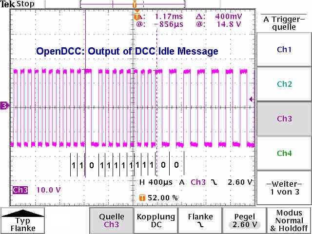
Figure: The openDCC output signal
The ACK detector
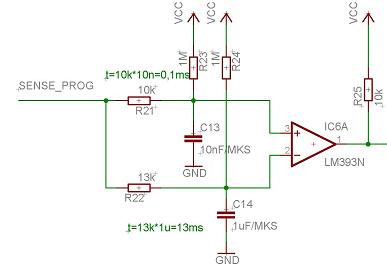
According to RP 9.2.3 a locomotive decoder in service mode should send back an acknowledge signal. This happens by the fact that the current is raised for a short time by 60 mA. This rise causes in the sense input of the programme a voltage drop. Following a suggestion of Martin Pischky the voltage drop is fed to different RC networks. Normally the voltage on the negative input of the comparator is approx. 11mV higher. By a change in voltage on the lower network needs clearly needs a longer time to follow the input. The comparator detects, hence, a short positive pulse with the increase of the voltage. This pulse releases an interrupt (active low) in the processor.
A high-pass filter circuit according to http://www.geocities.com/CapeCanaveral/Lab/2459/ACKDET02.HTMM would also have done the job. I have not taken the internal comparator of the ATmega because off its max. offset voltage of 40mV.
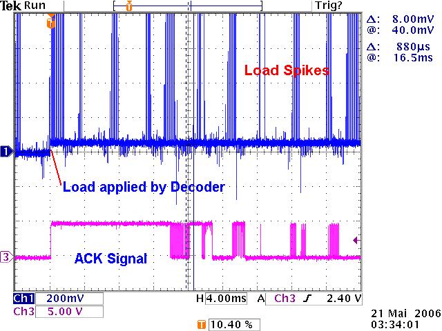
Here you can see the signals; on top is the signal SENS_PROG. At each change of the DCC signal, there will flow a high current for a short time. This will be filtered by means of an extra capacitor of 10nF at the input of the ACK-comparator, 10nF between pin 2 and 3. On the bottom the signal ACK_DETECT were you clearly can see the approx. 14ms long ACK pulse; if the RC network comes to a new level, overlapping of the switch pulses, so, the back edge of the signal ACK_DETECT has been "unravelled". ACK is recognized from a current rise of 50 mA (in accordance with the norm of 60 mA).
PC interface
Here the usual MAX232 or LT1081 is used for level translation. Newer variations need, as a rule, smaller or no capacitors, in this case simply the C's do not have to be equipped. In the layout 1 and 16 two vias are positioned beside the pins 1 and 16. In this case a LT1080 may also be used. This circuit is pin compatible, nevertheless, but has a 18-pin package.
Hardware handshake through CTS is supported. +10V on CTS (pin8) will allow data transfer in the direction of OpenDCC. RTS is connected to pin 7;
A USB interface is an alternative by using FT232RL. This component emulates a RS232 interface on the USB-bus; the secondary interface corresponds to RS232, indeed, with TTL level translation, so that a direct connection with the ATmega is possible. This chip with accompanying driving resistor is on the board in SMT (SO28). In case the USB-interface is used the driver from www.ftdichip.com must be installed, both jumpers JP5 and JP6 must be set to position USB, otherwise both straps must be in position RS232. Who has only one interface, can substitute the straps JP5 and JP6 by means of wire.
For the V1.3 these jumpers are only present on the board as strap wires, please pay attention to circuit diagram and part description on circuit diagram.
Keys and LEDs
All LEDs are 2 mA types; these can be driven directly from the ATmega outputs. One can equip the LEDs alternatively on the main board (bent forward) or on the front board. On the keys a RC network is planned to debounce these keys; this does not need to be equipped; the necessary pull-up is programmed with the ATmega and the debouncing is done by SW.
Booster
The H-bridge driver L6206 can output a theoretical maximum current of 2.8A. Indeed, this is limited by the power dissipation, which must flow away. On the layout are cooling surfaces, with this a thermal resistance of 44K/W is possible with on board soldered L6206. If one allows an increase in temperature of 90 degrees, no more current than 1.5A can be outputted for save operation.
The heat dissipation occurs basically through the groundpins, therefore a suitable cooling metal strip (copper strip) should be soldered in the hole row crosswise to the L6206. As a substitute solderpins and/or a small board strips are also possible. STM assumes for a cooling surface with 6cm2 copper a heat transfer of 44 K/W. In addition, one should stick on the package a heatsink to improve the heat transfer.
Indeed, other case kinds (PowerSO36) would have better heat dissipation and therefore better performance, but the problems is that it is very difficult to solder this package by hand.
The internal overcurrrent switch off circuit is equipped with a 15k reference resistor, this activates the switch off at approx. 1.5A. With capacitive loads (e.g., very much long wires (> 20m)) it is possible that the overcurrent circuit already responds because of the discharge of the output capacitance. In this case it is necessary to connect an external booster.
Please pay attention when choosing a box for good airflow. (drill some holes :-)
Please note: the track output is not connected to ground, but switches between around GND and VCC. By the application of occupation feedback encoder modules pay attention to potential mass loops!
S88:
The S88-bus is equipped with 74AC244 busdrivers. Every S88 string has its own clockdriver. To avoid sharp transitions a RC network is placed in the clock output, at the end of the wire a pull-up should be used of about 330 ohms connected to 5 V.
These are connected to the usual connectors (6-pin head) or alternatively a RJ45 socket is equippable. With this connector the S88 bus can be wired by means of CAT5 cable. From V1.4 and up the connections are following the standard S88-N.
Additionally, S88-N allows the transmission of RAILDATA, hereby using a buffer '125; to be able to report back a possible programmer-ACK on the S88-N the RESET tristate was made switchable. These options are not necessary for the normal S88 operation. Notes:
- in the V1.2 or V1.3 this cable allocation was used.
- Adaptors for existing modules are relatively simple made with MEB 8-8 (reichelt.de). This is a RJ45 socket with 70 mm of cable connections.
Connectors (Types)
Connection to the tracks is made by means of WAGO 734-164 and accompanying connector 734-104 (e.g., www.reichelt.de). As a substitute a 4-pole screwterminal (RM 5,08) can be also be used.
Connector for power supply: usual low voltage DC plug, e.g., Bürklin 40F140, (0338-8230-00), type AMP 5202550 (-,74), In addition a suitable plug is 40F120. As a substitute screwterminal can be also equipped here.
Connector for S88: RJ45: AMP 520251-4, Bürklin 73F558
Wish list and enhancements
-
Of course a simple box can not cover all wishes and the respective predilections
and needs have passed away.
The following wishes to an enhancement that have appeared up to now:
- Support Loconet
- Ethernet, as SRCP Server
Hardware Change Log
-
from V1.3 to V1.4
- RJ45 according to S88-N.
- Buffer for raildata added.
- Reset tristate possible
- switch between USB and RS232 through jumper
- SJ4 on comp. side from V1.2 to V1.3:
- Rotated RJ45 connectors
- More holes on front panel keyboard
- Added C44 (10nF) at IC6
- Changed value of R19, R20 from 10k to 2k2