Assembly instructions to open decoder (var. 2)
Introduction
- Before starting, the usual cautions: electronics soldering iron (not more than 300W ;-),
appropriate solder (not a Tiffany-lead solder),
diodes and capacitors properly polarized (small line in the layout or +),
ICs are static risk, in short, if you never built a circuit, you should not start with this one.
The exact values of resistors and C's are not critical in general.
Note: Variant 1is easier to build.
Procedure
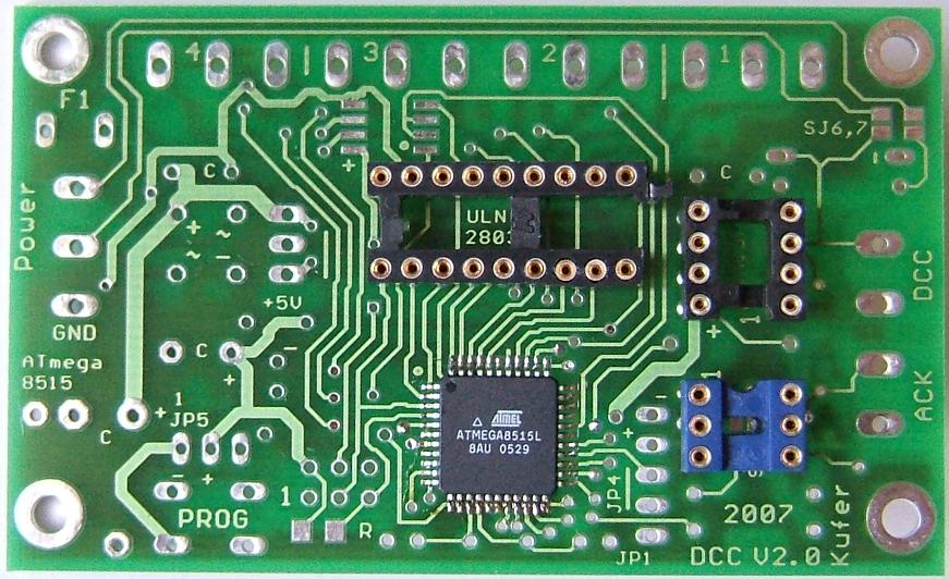
The ATmega8515 (in 44-lead TQFP housing, pitch 0.8 mm) should first be mounted on the component side.
- Recommendations for soldering the processor:
The ATmega is available in 44-pin package with 0.8 mm pitch.
Take a first corner pin on the PCB and put a bit solder on it.
Then place the chip on it and heat and sold this pin.
Thereafter the chip is exactly positioned on the pads.
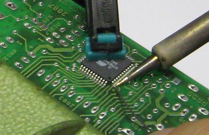
Now you can solder the other pins - 0.5mm fine solder and a thin soldering tip are helpful ;-).
Do not panic if pins are shorted circuited with solder: let cool the solder a bit and then take away the excess with desoldering braid.
Finally. Sockets, resistors, ICs, connectors and capacitors are mounted.
Special notes for Optocouplers OK3:
If 6N137 is used instead of 6N136, then a additional connection between pin 7 (enable) and pin 8 is required. This connection is not in the layout.
If 4N25 (6-pin housing) is used instead of 6N136 (8-pin housing), then pin 1 of 4N25 has to be placed on pin 2 of the layout.
Pictures of the assembled board
Commissioning and testing
- After the assembly, check again visually everything and remove residuals with alcohol.
Now apply voltage for the first time (from a regulated DC power supply, current limit fixed to 50mA).
Check the 5V and the current consumption. If the processor is already programmed, then the LED should flash rapidly 5x times, then take a break (total cycle time of 2s). After pressing the programming button, the LED should stay continuously illuminated. This initial control indicator 5-flash is switched off after programming the address.
Processor Programming
-
Once the hardware is completely built, the processor must be appropriately configured and loaded with the firmware.
This can easily be done with a homemade adapter (a few resistors and diodes, an RS232 connector and 6-pin connector)
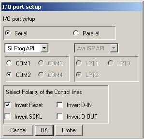
and a programming tool. As a free programming tool, you can use for example
ponyprog.
- Chip Configuration: how the chip will behave (running frequency, voltage, start conditions).
- Program: What program the chip should execute, eg OpenDecoder.hex
- EEPROM: predefined data which are stored in chip, for example, OpenDecoder.eep
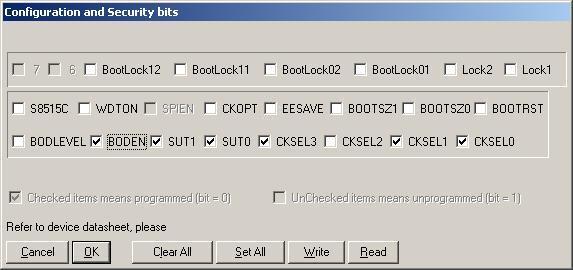
- Chip Configuration
Important: Before configuring the chip please disconnect external outputs 6, 7 and 8. (programming does no harm to connected LEDs, but if point drives are connected they will toggle together with the programming, makes a lot of noise and stresses the output drivers!)
The Atmel ATmega8515 has several options for timing and various boot modes. These are set with the so-called fuses. They can be selected in the menu item Command->Configuration . For OpenDecoder2 processor operations (internal RC oscillator), the following fuse bits are to be set to:Fusebits CKSEL3...0 =0100 Tick CKSEL3, CKSEL1 and CKSEL0 means usage of internal RC oscillator at 8 MHz CKSEL3...0 =1110 Alternative: Tick only CKSEL0 means Brownout Detector enabled with 10MHz crystal SUT1..0 =0 0 Tick SUT1 and SUT0 (Power Up Delay) EESAVE =1 No check mark in EESAVE means EEPROM contents will be overwritten during the upgrade. BODLEVEL =0 Checkmark means threshold at 4V, no checkmark means threshold at 2.7 V (requires ATMEGA8515L) BODEN =0 Tick, Brown Out Detection enabled -
Important: Please perform this operation very carefully and do not simply go with trial and error.
If the chip is configured to external clock and no external clock is connected to XTAL1,
then you can not talk to the processor anymore.
- Program:
To load the program open opendecoder2.hex, then transfer the program with the command write program to the atmel avr. Of course, the program file should fit to the above specified processor frequency. - Data (EEPROM):
Now we need to write the data into the chip. This is done with EEPROM file. Please choose .eep as extension when loading the data file.
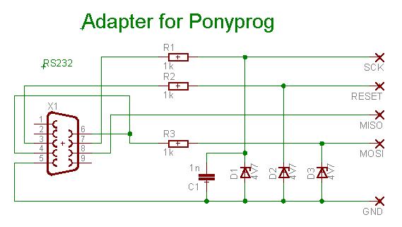
Note: With this adapter, the reset has to be marked as inverted in the Ponyprog configuration.
Connect this adapter to JP2 and program the processor. After programming the adapter can be removed again. This adapter can be used to program other processors as well.
Select the ATmega8515 AVR family chip in the programming tool.
When programming the following three things are stored on the chip:
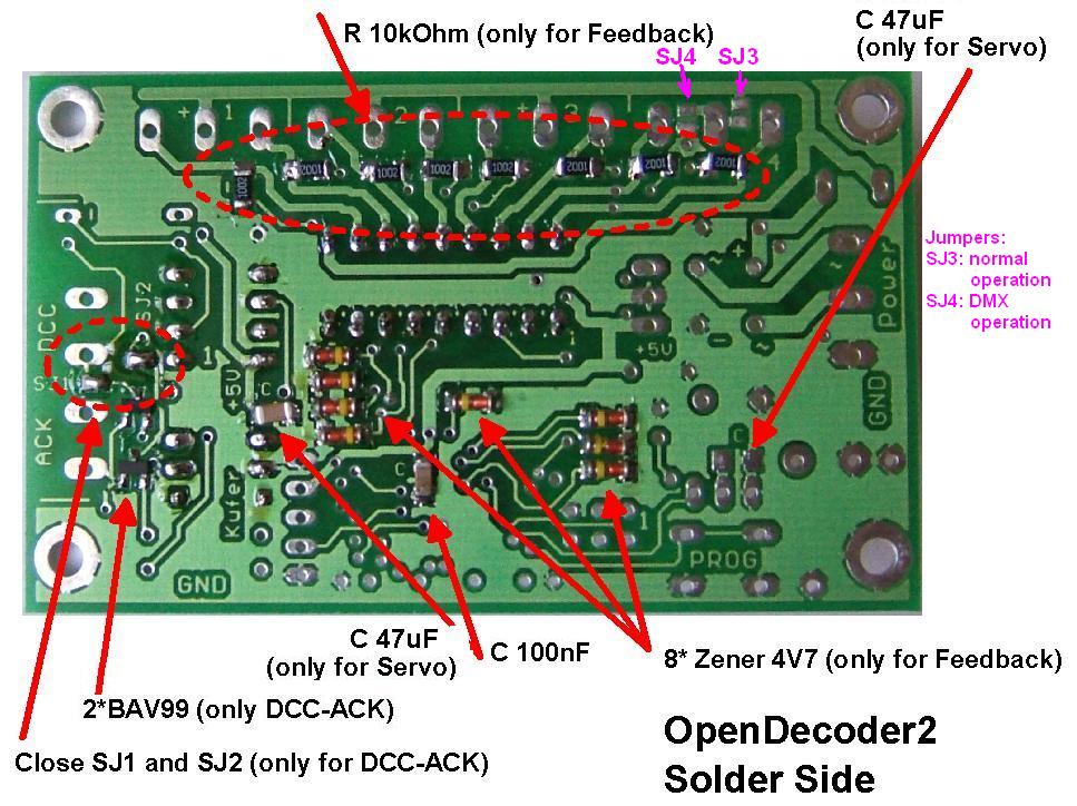
Options / jumper / solder bridges / changes:
- Quartz:
Optionally, a conventional HCU49 quartz can be used - the processor must be fast enough and the loaded program must be adjusted and compiled for this frequency. For quartz, the capacitors C4 and C5 are needed. - DMX Interface:
When IC1 (RS485 Drivers) is fitted, then X5 is omitted (same placement area on board).
In this case, SJ4 has to be be closed and SJ3 remains open - the middle pin of X6 is connected to GND. - Feedback:
If no feedback response (sensed with by end stop contacts) is required, then the Zener diode D2 to D10 (Melf) and the SMD resistors on the bottom side of the pcb should be eliminated. - ACK (CV programming):
If this is not needed, OK4, R13, R14, D14 and D15 (BAV99 on the solder side) can be omitted. - SJ1 and SJ2:
If they are closed, the feedback (acknowledge pulse) and the DCC input is coupled. This enables DCC-programming (CV values) of the decoder. (Of course, the corresponding components must be fitted). - SJ3 and SJ4:
These solder jumper allow to connect the middle pin of X6 either to +15V or to GND. For all normal applications SJ3 has to be closed and SJ4 let opened: they are inverted only with DMX. Under no circumstances should both be closed - SHORT! - SJ5:
This jumper is closed, if optocoupler CNY17 used instead of a PC817 one. Note: in this case, cut the connection between pin 4 and 5. - SJ6 and SJ7:
If they are closed, then the DCC input and the power input are connected. DCC is then connect to X2. - Power supply:
If a servo has to be powered with OpenDecoder2, the 5V regulator has to be cooled.
Versions and changes
-
Version 2.0:
- 12.04.2007: Value of R2, R4, R6, R7, R9, R10, R11, R12 changed from 10k to 22k
- 21.04.2007: added transistor T1 (BC560 or BC860) as emitter follower to create the correct current for DCC ACK..
What to do if it does not work?
-
At first, stay cool :-)
- Control all devices, whether the right component is at the right place and with the right polarity. This should have been done before switching the board on!!
- Visual inspection of solders and conductors - preferably with the optician microscope.
- Control the quality of the 5V power and current consumption
- Checking whether the programming works - and if yes read it back again with Ponyprog. Check the EEPROM as well.
- Control the reset line (should have a level of +5V) and the clock oscillator (if external crystal):
XTAL2 generate a 8MHz signal.
A freshly loaded processor (no address is programmed) flashes -x-x-x-x-x-----x-x-x-x-x----. The five flashes are quite fast, total cycle time is 2s. - If the the processor doesn't flash, but is reacting to pressing the key, the EEPROM content is probably not written.
- Does the polyfuse get hot? Then there is a short circuit on one output.
- If so far everything looks good, but the decoder does not respond to DCC: please load a test program with outputs activated and check the outputs. (Control: R15 and C11 are not equipped - n.f. = 'not fitted')
Then check the following things: